PCB Design Services That Prevent Costly Failures


Meet the Engineers Behind Your Circuits

JiteshJitesh
A PCB design engineer experienced in multi-layer board design, component placement, and circuit optimization. Proficient in stack-up planning, grounding strategies, and thermal considerations to ensure designs remain stable, manufacturable, and reliable across prototyping and production stages.


DarikaDarika
A signal integrity specialist focused on high-speed PCB design and noise reduction. Skilled in impedance control, differential pair routing, and EMI mitigation, ensuring consistent signal performance in high-frequency circuits such as DDR, RF, and communication systems.


HemantHemant
A hardware validation engineer responsible for pre-production testing and design verification. Experienced in identifying layout flaws, electrical inconsistencies, and manufacturability risks early to help reduce re-spins and ensure boards perform reliably under real operating conditions.

With Tools That Strengthen Layout and Validation


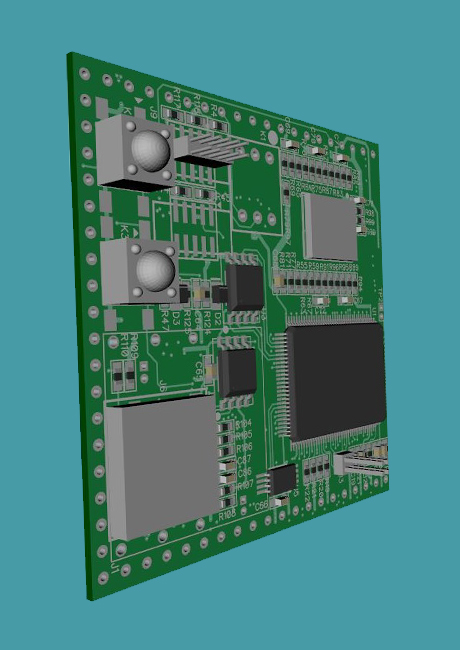
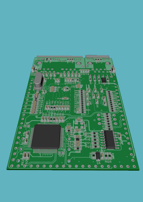
A Closer Look at Our PCB Design Expertise
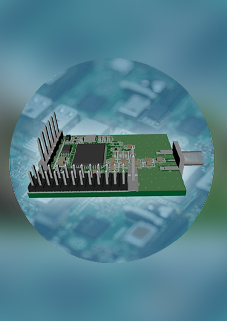
Wireless Boards
- A set of board, including MIST1413 (Temp, Light, Humidity Sensor) with SPI, Analog, and IRQ interfacing
- PIR (Passive Infrared Motion Sensor), SHT75 (humidity & temperature sensors), NTC for temperature sensor
Technologies Used
Estimated Time
4 weeks
Agriculture PCB
- Boards designed for wired & wireless value controlling
- Temperature, humidity, light & CO2 level monitoring boards
Technologies Used
Estimated Time
6 weeks
Home & Building Automation
- A set of boards used in security, home/office/building automation
- Used NXP’s LPC1768 and LPC1769 on board
Technologies Used
Estimated Time
6 weeks
Not Just Schematics or Components

At higher speeds, signals do not behave ideally. Poor trace routing, impedance mismatch, or incorrect layer stack-ups can distort signals, causing data loss or unstable system behavior. Precision layout ensures signals travel cleanly across the board without interference or degradation.

Electromagnetic interference is one of the most common reasons PCBs fail compliance testing. Inadequate grounding, improper shielding, or poor component placement can cause emissions that violate regulatory limits. Well-engineered layouts reduce noise and improve electromagnetic compatibility from the design stage itself.

As components become denser, heat dissipation becomes a critical constraint. Poor thermal design can lead to overheating, reduced lifespan, or sudden system failure. Effective PCB design distributes heat efficiently through copper planes, vias, and component placement strategies.

A design that works in simulation may still fail during fabrication. Issues like incorrect spacing, drill tolerances, or unsupported geometries can lead to production defects. Design for manufacturability ensures the board can be fabricated consistently without rework or yield loss.
With Our 5-Step PCB Designing Process
Every reliable PCB starts with a logically sound schematic. VE’s PCB design engineers define circuit behavior, component relationships, and electrical constraints while accounting for real-world operating conditions to ensure the foundation is accurate before layout decisions introduce complexity.
The layout stage determines whether a design will actually work. Your PCB design specialists at VE then translate schematics into physical board layouts using EDA tools, optimizing trace routing, grounding, layer stack-ups, and component placement to maintain signal integrity and reduce EMI risks.
Next, the designs are validated against fabrication constraints before manufacturing begins. VE’s offshore PCB designers coordinate with trusted vendors or your preferred manufacturer, ensuring design files meet production tolerances, reducing defects, delays, and inconsistencies during board fabrication.
Once fabricated, components are mounted with precise soldering processes aligned to design specifications. Proper assembly ensures electrical connectivity, minimizes defects such as cold joints or misalignment, and prepares the board for functional validation under real conditions.
Finally, testing verifies whether the board performs as intended under operational conditions. Your remote PCB designers conduct functional, electrical, and reliability checks to identify issues related to signal behavior, thermal stress, or manufacturing defects before the board moves to deployment.

Start With a Free Trial
Share your requirements and our team will help you get started quickly.- No credit card required
- No long-term contracts
- Cancel anytime
Trusted by Teams Building Reliable Hardware

The skills and contributions of VE’s engineer have played a key role in improving our product.
Harris Shallcross
Senior Electronics Engineer, Circuit Mind, UK
The biggest advantage of hiring VE’s resources is the high level of comfort and trust.
James Oliver
CEO, Oliver Technologies, USA
VE engineers’ work ethics and commitment are high, and it felt they are a part of my team.
Nick Ray
Director, Priva BV, NetherlandsRead Our Blogs on Hardware Design & Development

The Architecture of Embedded System Models in Real Time
In a world where your home adapts instantly according to your needs and your car predicts your every move, real-time embedded systems play a crucial role...
Read More >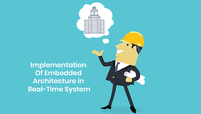
Implementation of Embedded Architecture in Real-Time System
Embedded real-time operating systems are present today in many devices that we use for our day-to-day functioning as well...
Read More >
Embedded Product Development Life Cycle: Four Main Steps
Today, almost every modern application comes with an embedded system. From the latest smartphone, smartwatches...
Read More >PCB Designing Questions
4500+ Clients in 48 Countries Have Accelerated Their Business Growth with VE’s Specialists. You Could Be Next!