Highly Complex PCB Layouts within Specified Time & Budget

Exactly What Our Numbers Reflect

In-House Developers
50+

PCB Design Engineers

Successful Projects
2800+

Verified Components

Client Retention Rate
98%

Prototype Success Rate

Certificate Icon
12+

Years’ Industry Experience
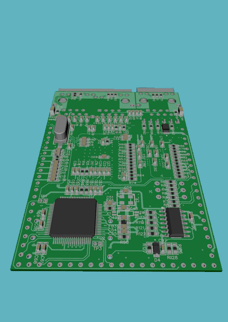
Welcome 50% More Energy-Efficient PCBs With

Comprehensive PCB Design Services

Increase Your Chances to Succeed in Field Trials

With Our Latest PCB Design Tools

Professionals Ready to Fast-Track Your Projects

Our Pre-Vetted PCB Design Engineers

Get A Glimpse of Our Experts'

PCB Designing & Prototyping Proficiency

Not Just EMC/EMI Compliant PCB Designs

But Benefits Meeting Your Business Needs

Free Trial Tax Preparer

Kick-start your project straightaway with our popular No-Obligation, No-Payment up to 3-day Free Trial. Continue with the same resource if satisfied.

Free Recruitment

Our free, quick, bespoke hiring process helps you save on not just expensive local recruitment fees but also lengthy waiting periods to hire just one resource.

Zero Overheads

Get your own 'remote workplace in India’, do away with pesky issues such as HR, Admin, Payroll, etc. and only pay your offshore PCB designer’s salary.

Data Security QuickBooks Expert from India

As an ISO27001:2013 certified and CMMiL3 assessed company, VE assures its clients of breach-proof data security and confidentiality at all times.

Design Complex Circuits in 50% Lesser Time

Our 5-Step PCB Designing Process

Schematic & Circuit Design

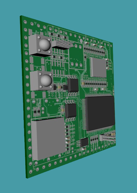
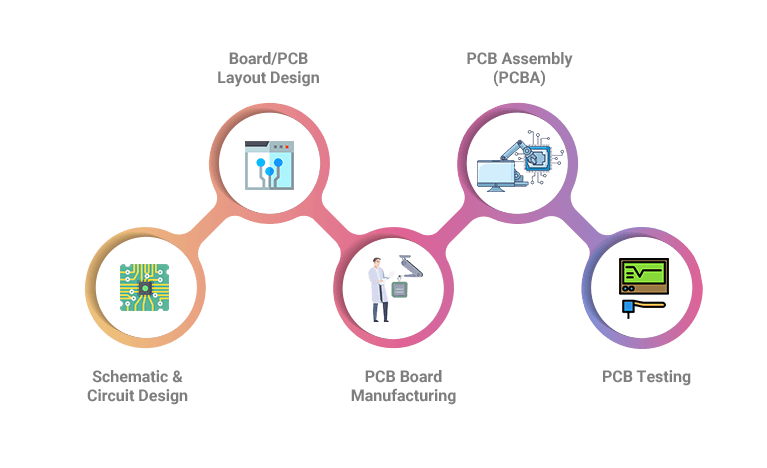
VE’s expert PCB designers will start drawing the simple 2D circuit design displaying the connectivity and functionality between distinct components.

Our printed circuit board design engineers will utilize the schematic capture tool or EDA software to create the PCB layout and show where the components will be placed.

Your offshore PCB designers at VE then get your PCB manufactured by a trusted vendor and deliver a top-quality PCB within the stipulated time. You can also opt to get your PCB created by your preferred manufacturer.

Post PCB fabrication or manufacturing, VE’s professional PCB design engineers will mount the components of your board on the bare board with the soldering method.

As one of the top-rated PCB design companies in India, VE offers PCB testing services during and post-development to examine the board’s capability to perform its expected operational functionality.

Our 5-Step PCB Designing Process
Staffing Plans to Match Your Market Demands

Our Custom Hiring Models

3500+ Global Clients Bank on Our Services

Nick Ray Director, Priva BV, Netherlands

VE engineers’ work ethics and commitment are high and it felt they are a part of my team.

Nick Ray
Director, Priva BV, Netherlands
VE's Client Testimonial - Jonathan Torkelson - Embeddetech Inc.,President, Tulsa, Oklahoma, USA

Virtual Employee’s scalability is amazing and I highly recommend their services.

Jonathan Torkelson
President, Embeddetech, USA
James Oliver CEO, Oliver Technologies, USA

The biggest advantage of hiring VE’s resources is the high level of comfort and trust.

James Oliver
CEO, Oliver Technologies, USA

You Are Wise to
'Look Before You Leap'

And, so, here's...
A deal like no other. 1 Week Free Trial Icon
No card details required Icon

No card details required.

Senior architect’s assistance Icon

Senior technical architect's assistance.

Zip Icon

Keep all the work. It's yours.

Share Your Requirement

Get Valuable Insights to Stay Updated

Read Our Blogs on Embedded Development Services

Implementation of Embedded Architecture in Real-Time System

Implementation of Embedded Architecture in Real-Time System

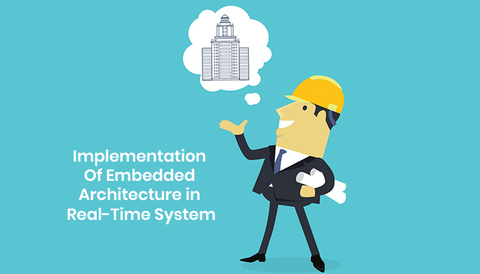
Embedded real-time operating systems are present today in many devices that we use for our day-to-day functioning as well...

Read More >
Irfan ahmed
By Irfan Ahmad Feb 14, 2023
Embedded Product Development Life Cycle: Four Main Steps

Embedded Product Development Life Cycle: Four Main Steps

Today, almost every modern application comes with an embedded system. From the latest smartphone, smartwatches...

Read More >
Arnab
By Arnab Bannerjee Oct 26, 2021
Benefits Of Offshore Software Development Services

Benefits Of Offshore Software Development Services

In this fast-paced digital world, the concept of software development has drastically changed as numerous...

Read More >
Daya
By Daya Mukherjee Sep 13, 2022
Have More Questions? This Might Help!

FAQs on Our PCB Designing Services

If you are looking to outsource PCB design services to India, you need to make sure that:
  • The PCB design engineer can efficiently address issues related to PCB design like signal integrity and EMC concerns.
  • Your PCB designer is capable of creating designs valuable for manufacturing, engineering, and testing processes.
  • The printed circuit board designer can recommend definite requirements for your specific board like two-sided or single production and requirement of surface mounts.
Our PCB designers in India have the following qualification:
  • A solid academic background in sketching, design, and Computer-Aided Design (CAD) technology, with a similar background in allied software.
  • Profound knowledge of how to operate the software to design the most accurate and high-quality PCB designs for your product.
  • Capability to examine designs exhaustively to recognize minor flaws that can disturb the functionality of your product.
At VE, we take the rigorous recruitment approach to develop a strong slate of PCB designers and make sure we deliver only high-calibre talent to your business. Virtual Employee follows a triple-vetting process so that you don’t even need to train your hired PCB design engineers. Hire PCB designers from VE today and see for yourself how they can transform your business.
At VE, you can ask our resources to design the following types of PCBs:
  • Single Layer PCBs
  • Double Layer PCBs
  • Multilayer PCBs
  • Rigid PCBs
  • Flex PCBs
  • Rigid-Flex PCBs
Effective PCB routing can be achieved from best component placement. This means after component placement (as per circuit) the PCB should look good, component aligned, and even top/bottom silks properly placed. The PCB routing best practices followed by our PCB designers include:
  • Decoupling capacitors must be placed as close as possible to the Vcc pin.
  • The power via should be placed in between decoupling cap and pad.
  • Try to use multiple GND via for ICs, it will give good return path.
  • Analog and digital signal/GND planes should be non-overlapping.
  • Place termination resistors near source of the signal.
  • Try to use single solid GND plane.

Build Problem-Solving Products – Hire PCB Designers from India

PCBs or Printed Circuit Boards are electrical and mechanical layouts illustrating the electrical connections within separate components. A variety of components like resistors, batteries, capacitors, transistors, and LEDs are generally soldered to the PCB to keep them in position and enable smoother device function. A PCB layout design offers plenty of info about the fundamental design components and the circuitry amongst them. PCB designs or layouts are quite valuable, particularly in the electrical and mechanical industry, in the design or production of equipment that is technologically advanced...

Why Should We Outsource PCB Design Services to India?

When you hire PCB designers from India, you can enjoy peace of mind by saving ample PCB prototyping and development time. Also, you can obtain high-quality electronic design services from extensively experienced and skilled individuals without breaking a sweat.

Save Above 50%

If you hire PCB design engineers from India, they usually work based on a contract. The top-rated PCB design companies in India like VirtualEmployee.Com offer custom hiring solutions, which ensure the finest level of service without exceeding your budget. As per reports, businesses who choose to outsource PCB design services to India can save up to 50-70% and build futuristic products.

Skilled PCB Designers

Leverage the expertise of professional PCB designers from India who have worked across a variety of industries. Virtual Employee has helped several businesses in building value by delivering PCB design engineers with profound knowledge and experience. VE’s PCB design experts in India can easily understand your industry and build top-quality products without a glitch, owing to their technical expertise.

Different Levels of Experience

In India, you can find PCB designers with diverse skill and experience levels. At VE, you get to handpick the desired resource according to your project’s requirements, which allows you to do away with unnecessary hiring expenditures and failures.

Constant Monitoring

When you outsource PCB designing services to India, you can track the performance of your remote PCB design specialist regularly and provide your valuable inputs every once in a while, for reducing the recreation and prototyping time and cost.

Ultimate Flexibility

In India, you can hire the best resources without paying steep recruitment fees. Your PCB design partner in India such as VE offer flexible hiring models to satisfy your custom recruitment needs and scale up or down whenever required.

What are the Advantages of Outsourcing PCB Design Services to VE?

Talking about PCB designing, there are several significant factors that you should consider. These aspects may comprise the kind of PCB to utilize, the type of software to employ, and many more.

If you are planning to outsource PCB design services to India, you can get complete support and experienced resources to design printed circuit boards that match your needs. A majority of PCB design and development companies are extensively experienced and profoundly skilled in their industry.

This profound knowledge and experience can reflect in your PCBs if you collaborate with the right PCB design company. Also, you can enjoy various advantages of outsourcing PCB design services to a partner like Virtual Employee:

Technical Proficiency

At Virtual Employee, you get access to unmatched technical expertise in the form of offshore PCB designers. With VE’s experienced PCB design engineer on your team, you can make sure that your components and layouts perfectly match your needs. Whether you require assistance related to concept ideas, prototypes, or schematics, you can readily avail the expertise of your hired PCB designers.

Product Optimization

A primary advantage of partnering with a top-rated PCB design company in India is that VE’s PCB designers can flawlessly assess your plans and identify the facets that need improvement. Our PCB design specialists from India can even suggest the omission of unnecessary parts for added savings. A renowned PCB design company like VE can also evaluate your schematics and pre-existing boards to analyze how your product can be enhanced by optimizing the design and helping you save both money and time in the long run.

Design Error Reduction

If there’s a design issue in your PCBs, VE’s PCB design experts from India can offer the much-needed knowledge to eliminate any design issues. Our dedicated PCB design engineers can come up with a new perspective on problems that may assist in resolving products quickly. You may come across design flaws every once in a while, but it’s vital to decrease design flaws to build a technologically sound product for the user.

Quicker Prototyping

Prototypes are eventually critical for PCB development, and it’s crucial to build prototypes at the right time to stay consistent. If you have fresh ideas and require developing a prototype quickly, VE’s PCB design experts from India can do the needful in no time.  Since you will be collaborating with PCB design specialists, you can be confident that they will have techniques in place to carefully plan and thoroughly test your PCB to secure peak functionality.

98% of PCB design prototypes made by VE’s embedded team have succeeded in field trials. Sounds too good to be true! It’s certainly a rare feat for any PCB outsourcing company in India. According to a study by Mentor Graphics, layer counts on printed circuit boards have stayed almost the same, but the area has reduced by 33% and the density has risen by 25%. Your projects can succeed only when the design and development processes are extremely streamlined.

This is where partnering with Virtual Employee, one of the most reputed PCB companies in India, can make all the difference. When you hire an experienced and highly skilled Printed Circuit Board Designer from VE, you get access to 2800+ verified and tested PCB components and footprints, which save a lot of time in prototype development by minimizing human error.

We also follow the best industry standards. For instance, component libraries are centrally built and managed, and work-in-progress files are stored securely. Apart from this, you get EMC/EMI-compliant PCBs. This gives VE’s PCB Engineers an amazing 98% success rate in field trials.

3500+ Clients in 48 Countries Have Accelerated Their Business Growth with VE’s Experts. You Could Be Next!